YBa2Cu3Oy (YBCO) belongs to a class of oxide materials collectively referred to as “high-Tc (critical temperature) superconductors (HTS),” i.e., materials that exhibit superconductivity above the boiling point (77K) of liquid nitrogen. However, as these materials are typically brittle, in order to be used for potential applications they have to be processed into a useable form, such as long-length wires or tapes. While this is not an easy feat, advances in materials processing technology have enabled the fabrication of thin layers (micrometer thickness) of YBCO on flexible metal tapes with buffering metal oxides, known as coated conductors.

The high cost of materials processing, however, is a main challenge that needs to be hurdled in order to make coated conductors a commercially viable alternative compared to conventional copper. There are two routes that can be explored: investigation of low-cost processing techniques such as solution-based film deposition methods, and enhancement of current-carrying property of the film, which will also cut down the cost drastically (i.e., fabricating a thinner layer with high current-carrying performance is more economical than a thicker layer but with low current-carrying performance). In simple terms, this current-carrying property is controlled by the effectiveness of existing defects in the film to “pin” or prevent the movement of magnetic vortices, the movement of which gives rise to electrical resistance and thereby limits the amount of supercurrent through the film.
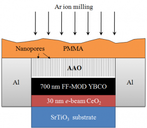
In line with these efforts, researchers from the National Institute of Advanced Industrial Science and Technology (AIST) and the University of Cambridge studied a novel method for enhancing the current carrying properties of YBCO thin films fabricated using a low-cost, non-vacuum method of metalorganic deposition (MOD). In a recent publication [1], Dr. Katherine Develos-Bagarinao and co-authors explored a novel, top-to-bottom method for introducing nanosized defects (nanodefects) into ~700 nm, fluorine-free MOD-grown YBCO thin films prepared on CeO2-buffered SrTiO3 single crystal substrates. In this method, nanoporous anodic aluminum oxide (AAO) membranes, commonly used for the fabrication of a wide variety of nanostructures, were used as etching masks for YBCO thin films, and subsequently exposed to argon ion milling. The membranes had pore sizes of 90–100 nm arranged hexagonally with an interpore spacing of ~100 nm. This is similar to the method previously explored in the University of Cambridge wherein AAO templates were prepared directly on Nb superconductors [2]. Unlike Nb superconductors, however, it is not straightforward to prepare AAO directly on YBCO, because the anodization process requires an acidic medium which is highly corrosive to YBCO. The solution to this dilemma is to use a free-standing AAO membrane which is sufficiently thin and mechanically supported by an easily etched polymethylmethacrylate coating. The schematic of the setup is illustrated in Fig. 1. This study represents the first attempt to use AAO membranes as a template for the processing of already grown YBCO thin films. After milling, the films were annealed at 450°C for 1 h in flowing oxygen to restore any oxygen lost through the milling process.

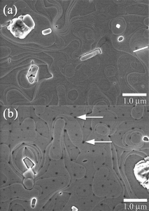
Evidence of the successful incorporation of the nanodefects into the YBCO thin films is shown by the subsequent evaluation of the films after milling. Figure 2 shows the typical scanning electron microscopy (SEM) images of the YBCO thin film acquired before and after milling, where the dark spots visible on the surface of YBCO correspond to the milled defects. Furthermore, electrical characterization of the YBCO films before and after milling revealed an enhancement in the critical current density (Jc), a very important parameter considered for the practical application of these materials. This represents the amount of current that can be passed per unit area of the superconductor; exceeding this value results to the breakdown of superconductivity. At 77.3 K and self-field (zero applied magnetic field), a moderate enhancement in Jc of ~50% was observed for the milled YBCO. Surprisingly, the introduction of nanodefects have inadvertently led to higher anisotropy of Jc in the presence of external magnetic field, i.e., Jc exhibited strong enhancement depending on the orientation of the external field with respect to the crystallographic axes of YBCO. Specifically, the authors noted that Jc is remarkably enhanced when the applied field is parallel to the ab-plane of YBCO. At an applied field of 1 T, up to twofold increase in Jc is observed for the milled YBCO film compared to the controlled sample, suggesting that the milled defects have given rise to oxygen disorder which affected the Jc behavior. This oxygen disorder has been confirmed by the evaluation of the in-plane microstrain of the films using x-ray diffraction.
Further details about the study can be found in [1].
References:
[1] Develos-Bagarinao K et al., Supercond. Sci. Technol. 25 (2012) 065005 (pdf)
[2] Dinner R B et al, Supercond. Sci. Technol. 24 (2011) 055017