Post contributed by Dr. Elmer Estacio, currently affiliated with the Far Infrared Center, University of Fukui. His area of research is on MBE-grown terahertz semiconductor emitters and development of high-speed terahertz time-domain spectroscopy techniques.
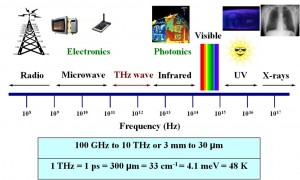
The terahertz (THz, 1012 Hz) frequency region bridges the gap between electronics (microwave band) and photonics (IR and visible light bands). Electromagnetic radiation having frequencies that fall within ~0.1 THz to ~10 THz is referred to as a THz wave or T-ray (see Box 1). Until recently, the THz regime has remained widely unexplored. In the past 2 decades, however, THz spectroscopy and imaging have been proven to be increasingly feasible for applications in pharmaceutical and semiconductor testing, environment sensing, medicine, and even law enforcement. This wealth of possible applications is primarily owed to THz spectroscopy being (1) sensitive to carrier dynamics of semiconductors and other materials without requiring low-temperature conditions; and (2) the “fingerprint” spectra of major biomolecules are located in the THz region and thus, building a comprehensive spectroscopic database for these complex molecules appears to necessitate THz science.
 |
| The electromagnetic spectrum showing the relative location of the THz band. It bridges the electronics and photonics regimes. |
The rapid development of THz science and its full commercial implementation is being hampered by the lack of robust and intense THz radiation sources. As such, one of the most important aspects of THz research is the continued search for intense pulsed THz radiation sources. At present, THz radiation from femtosecond (10-15 of a second) laser-irradiated semiconductors has been extensively studied, in line with the development of portable, easy-to-use, and intense pulsed THz emitters. Bulk p-type InAs (Indium Arsenide, a semiconductor material composed of Indium and Arsenic) is considered as the most intense semiconductor surface emitter while GaAs (Gallium Arsenide, a compound of the elements Gallium and Arsenic) has been used as substrate material for THz photoconductive antennas. Silicon, on the other hand, is an integral component in THz focusing optics. As such, efforts to possibly incorporate two of the most widely used semiconductor THz emitters into the highly-established Si technology could be crucial in integrating THz science into the mainstream semiconductor industry.
In a paper recently published in Applied Physics B journal, we demonstrated the generation of THz radiation from laser-illuminated GaAs and InAs thin films grown on Si substrates (GaAs/Si and InAs/Si), by molecular beam epitaxy (MBE). Results show that for these samples, THz emission is possible for both reflection and transmission excitation geometries, promising ease-of-alignment to expand the practical applications of these THz emitters.
Terahertz emission data from the reflection-geometry experiment showed that p-InAs and GaAs/Si emitted the strongest THz radiation (the bandwidth ranges from 0.2 to 1.5 THz) while InAs/Si emission was an order of magnitude less. The bulk GaAs emission is 2 orders of magnitude weaker than the GaAs/Si so it can be surmised that a GaAs film on Si enhances its THz emission 100 times. This enhancement is currently attributed to the existence of a strain-induced electric field at the GaAs-Si interface due to the lattice-mismatch between these two materials. This strain field causes the more efficient sweeping of the photocarriers across the interface, thereby enhancing the THz emission intensity.
Oscillatory features are seen for the thin film samples’ emission spectra and these are attributed to Fabry-Perot modes: an indication that the Si layer is significantly transparent to THz radiation. The THz radiation for the transmission-geometry case exhibited prominent Fabry-Perot modes in the emission spectrum of GaAs/Si, which are consistently absent in the InAs/Si sample. Despite GaAs/Si undoubtedly being the more intense thin film emitter, InAs/Si has a well-behaved THz emission spectrum and could be more suitable as a broadband THz source for spectroscopic applications.
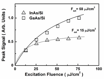
Excitation fluence saturation measurements (see Box 2) were also carried out and the comparatively low saturation fluence for InAs/Si is believed to be due to a slight difference in the THz radiation mechanism between these two samples. For GaAs, the electric field-driven drift current dominates the THz emission. However, InAs primarily emits due to a net current arising from the difference in the drift velocities of its electrons and holes. The latter mechanism occurs near the surface and is prone to the detrimental effects of carrier density buildup, thus resulting in quick saturation.
 |
| The excitation fluence dependence of the samples’ THz emission in the transmission geometry. The symbols are the experimental data while the lines are least squares fits to the expression, A/(1+Fsat/F), where Fsat is a saturation fluence fitting parameter. The best fit lines revealed saturation fluence values of ~15 mJ/cm2 and ~58 mJ/cm2 for the InAs/Si and GaAs/Si, respectively. |
These results demonstrate the feasibility of using GaAs/Si and InAs/Si thin films as intense THz emitters. Unlike bulk materials, thin films allow for numerous ways of optimization such as growth parameter improvements and even creating new thin film hetero-layer designs. Moreover, this work lends proof that incorporating well-known THz semiconductor emitters and Si into a single emitter wafer is possible and could help in hastening the commercialization of THz optoelectronics.
Details of the study can be read in “Intense terahertz emission from undoped GaAs/n-type GaAs and InAs/AlSb structures grown on Si substrates in the transmission-geometry excitation” by E. Estacio, et. al, Applied Physics B 103 (2011), pp. 825–829 (doi: 10.1007/s00340-011-4371-0)
This is the evolution of new technology with minimum budget and a fast traveling of data with minimum harm to body this could be an achievement in the science and thanks to the scientist and engg, who achieved this technology.Thanks for sharing.