K. Develos-Bagarinao
Energy Technology Research Institute, National Institute of Advanced Industrial Science and Technology, 1-1-1 Umezono, Tsukuba, Ibaraki 305-8568 Japan

Cerium oxide (CeO2) has been receiving great attention due to its numerous industrial applications, such as catalysts, fuel cells, oxygen sensors, among others. Moreover, cerium oxide thin films have been widely investigated as buffer layers for high-temperature superconducting YBa2Cu3O7-δ (YBCO) films as components for high-power applications such as fault current limiters, and passive microwave devices such as antennas and filters.
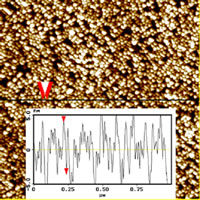
Cerium oxide is commonly used as a buffer layer due to its thermal stability at high temperatures required for the deposition of YBCO on sapphire substrates, and good lattice matching with YBCO. However, due to the lattice mismatch of cerium oxide with sapphire, epitaxial layers of cerium oxide are highly strained. Growth therefore proceeds via formation of 3D islands, and the typical as-grown morphology is granular and rough. Figure 1 shows a typical surface morphology acquired through atomic force microscopy (AFM) of an as-grown CeO2 film deposited by large-area pulsed laser deposition (PLD) method (Image size: 1 mm × 1 mm). Further studies indicated that YBCO films deposited on such as-grown cerium oxide are of low quality, particularly in terms of their crystalline properties and critical current density Jc. Jc is an important parameter because its value determines the maximum amount of current that can be passed through a superconductor without resistance. Our primary interest is on the optimization of these cerium oxide thin films as buffer layers to obtain higher values of Jc for large-area YBCO films.
 |
 |
| Figure 1. AFM image of as-grown CeO2 thin film grown by large-area PLD. | Figure 2. Typical AFM image of a CeO2 film after annealing. |
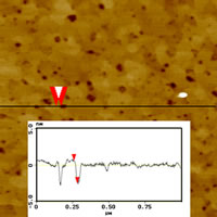
High-temperature annealing is a simple and easy method to modify the surface of cerium oxide from granular and rough to one that exhibits atomic flatness. Typical annealing is carried in a box-type furnace at ~1050 degrees Celsius in flowing oxygen. Experimental evidence showed that annealing the cerium oxide film prepared by large-area PLD results to very flat and continuous (001) nanostructures, and depending on the length of annealing time, nanopores will develop on the surface. Figure 2 shows the typical surface morphology and corresponding line profile acquired by AFM of an annealed cerium oxide film (Image size: 1 mm × 1 mm). Our studies indicated that the intrinsic properties of the cerium oxide film, which are dependent on the type of deposition method employed, have significant influence on the evolution of the surface morphology upon subjection to high-temperature annealing [1].
The more important question, however, is whether the surface modification of the cerium oxide buffer layer would have significant influence on the properties of the YBCO film grown on top. Compared to only as-grown cerium oxide, annealed ones have been proven as better templates for the subsequent growth of YBCO. From investigations of the defect microstructures of YBCO films deposited on cerium oxide-buffered sapphire, as well as cross-sectional TEM observations, additional dislocations in YBCO were found to be induced by the presence of nanopores on the buffer layer. The threading dislocations in the YBCO film, parallel to the c-axis direction, act as effective flux pinning centers which contribute to the increase of the critical current density Jc. These YBCO films deposited on annealed cerium oxide surfaces containing a high density of nanopores have indeed been shown to possess increased values of Jc’s [2].
References:
[1] K. Develos-Bagarinao, H. Yamasaki, Y. Nakagawa, J. C. Nie, M. Sohma and T. Kumagai, “Comparative studies of nanostructural and morphological evolution of CeO2 thin films induced by high-temperature annealing,” Nanotechnology, 18 (2007) 165605.
[2] K. Develos-Bagarinao, H. Yamasaki, and Y. Nakagawa, “Effect of surface modification of CeO2 buffer layers on Jc and defect microstructures of large-area YBCO thin films,” Supercond. Sci. Technol. 19 (2006) 873-882.